Home > Teams > Optoelectronics, Heteroepitaxy and Materials (OHM)
Optoelectronics, Heteroepitaxy and Materials (OHM)
Team coordinator Charles CORNET
The OHM research team studies the elaboration, and the electro-optical/electronic properties of new materials, compounds and devices (mainly semiconductors) for photonics and photovoltaics. To this aim, the research team benefits from several facilities, spanning from molecular beam epitaxy (MBE) of nano- or heterostructures to clean room devices processing, and several skills by using modelling and the study of structural, optical, electrical, electro-optical or functional properties. Research activities then begin with the understanding of materials at the atomic level and ends with photonic or photovoltaic demonstrators. These activities correspond to four research axes of the FOTON institute. A brief description is given in the following:
![]() Axis I: Devices and functionalities for optical communications
Axis I: Devices and functionalities for optical communications
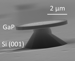
 The research team works on the development of laser sources with InP-based nanostructures (quantum wells, quantum wires or quantum dots). Both edge-emitting laser devices and surface emitting lasers (VCSELs) are being studied. This is done in collaboration with SP and DOP research teams. Integration of both active and passive photonic III-V devices on silicon, via the GaP semiconductor, is also considered in order to use optical non-linearities on-chip, for optical interconnects or THz generation.
![]() Axis IIIInnovative materials for photonics
Axis IIIInnovative materials for photonics
 The research team studies at the earliest stages the development of new materials and nanostructures for photonics and photovoltaics. Here, structural, electronic and optical properties of various materials are explored (e.g. hybrid perovskites, liquid crystals for photonics, carbon-based nanostructures, 2D or 3D materials, with or without quantum confinement). These studies allow assessing the potential of these materials toward their use in photonic and photovoltaic devices.
![]() Axis II & Axis IVTera-Hertz optics, optical sensors and coherent imaging
Axis II & Axis IVTera-Hertz optics, optical sensors and coherent imaging
 The OHM research team mainly develops here some vertical-emitting laser devices (being VCSELs or VECSELs) with InP-based quantum nanostructures for dual frequency lasing, frequency upscaling to the millimeter and THz domains, instrumentation or optical sensors, in collaboration with the DOP research team. Middle infrared resonant microcavities are also fabricated for gas spectroscopy. Finally, in a prospective approach, GaP for THz generation is also studied.
![]() Axis VAdvanced concepts for Photovoltaics
Axis VAdvanced concepts for Photovoltaics
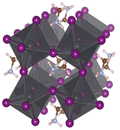
 The team works experimentally and theoretically for the development of new photovoltaic solar cells concepts. Especially, the very promising hybrid perovskites, a material of choice for tomorrow’s solar cells, are carefully studied within the research team. But other concepts such as III-V/Si solar cells or hot carriers solar cells, are also being developed experimentally and theoretically.
Equipment and skills available in OHM research team are part of the technological platform « NanoRennes », that joins together the technological equipment and skills of Foton-OHM (INSA) and IETR-MM (UR1). NanoRennes is a regional technological platform, dedicated to characterization and micro-nanofabrication tools, that is part of the CNRS national platform network. Nanorennes offers skills, expertise and equipment for the realization of collaborative projects, service provisions with academic or industrial partners.
Skills
The OHM research team is composed of INSA-Rennes and INSA staff, of 46 contractual or permanent members, including 24 senior scientists, 10 PhD students, and 11 technicians/engineers or administrative staff. Research activities of the OHM team mainly relies on the four following skills:
![]() Materials/crystal growth by MBE
Materials/crystal growth by MBE
![]() Clean room processing/devices
Clean room processing/devices
![]() Study of electro/optical properties
Study of electro/optical properties
![]() Atomistic simulations and device modelling
Atomistic simulations and device modelling
Equipment
The available equipment at OHM is listed below:
- Epitaxial growth reactors for Si and III-V materials (2 MBE, 1 UHV-CVD</acronym)
- ISO 4 / ISO 5 clean room of 120 m², including:
- UV photolithography experimental setup
- Stylus-based profilometer for thickness measurements
- Electron beam physical vapor deposition of metallic thin layers (Au, Ti, Pt, Ge, Pd, Ni, Al, Cr, ...)
- Plasma-Enhanced Chemical Vapor Deposition of dielectric materials - PECVD (Si, Si3N4, SiO2 ...)
- Chemical etching and/or plasma-assisted etching (RIE</acronym) of many different materials
- Rapid Thermal Annealing (RTA)
- Micro-wiring of devices (Au, Al)
* Experimental setups for optical studies:
-
- Experimental setups for emission wavelength from 0.4 to 5µm, with or without cryogenic facilities (from 10 to 400K), photoluminescence, electroluminescence, laser characterizations, and microscopy
- Ultra-short (130fs) laser pulses experimental setup covering the [0.4, 3]µm wavelength range
- Quantum efficiency measurements for solar cells
 FOTON-OHM team publications
FOTON-OHM team directory


