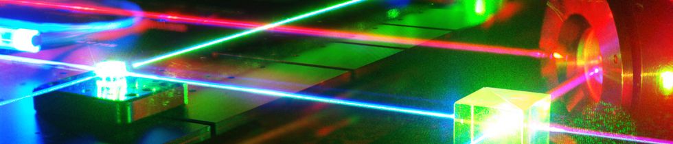
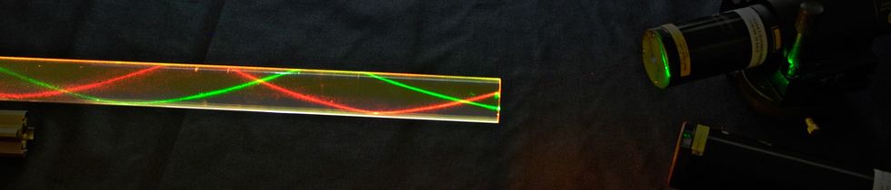
Foton-OHM Nanorennes site has particularly a great expertise in InP and Si based MBE materials growth, optical characterizations (from UV to IR), and photonic devices processing (lasers, resonators,…). The main facilities available are:
 Photolithography Photolithography- 2 spin coaters
- 2 UV mask aligner (Suss Microtec MJB4 et MJB3)
- Wafer size : < 3 inches
- resolution 0.8 µm
|
 Thin layer deposition Thin layer deposition
 Metal : 4 reactors Metal : 4 reactors
- E-beam evaporator Temescal
- Metals : Au, Pt, Ti, Ge, Pd, Ni
- Thickness control
- Wafer size < 3 inches, up to 6 wafers
- Homogeinity ( < 5%
- Joules evaporator Leybold
- Metals : Au, Al, In, Zn, Cu, ..
- Wafer < 2 inches
- Sputtering system Leybold
- Métals : Au, AuGe, Ti
- Wafer < 2 inches
- Sputtering system Alcatel
- Metals : Ti, Ti alloys
- wafers < 2 inches
Dielectric : 2 reactors
- PECVD Plasmatechnology
- Si3N4, SiO2 at 300 °C
- wafers <3 inches, up to 4 wafers
- Homogeinity : 5 %
- Sputttering system Leybold
- Si , SiN
- wafers < 2 inches
|
 Etching Etching
Wet chemicals (semiconductors : Si, InP, GaP, GaAs), organics (photoresists, BCB, ..), metals (Au, Ti, Al ..), and dielectrics (SiO2 ; Si3N4, ..)
Dry : 2 RIE reactors
- Plassys MG100
- SF6/O2
- wafers < 4 inches
- interferometric control
- Alcatel GIR 300
- H2/CH4/Ar
- wafers < 3 inches
- interferometric control
|
 Ovens Ovens
Hot plate under inert atmosphere (N2), T< 400 °C
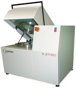
Rapid Thermal Annealing Jipelec
- Primary vaccum, inert atmosphere (N2/H2)
- T < 1300 °C, 150 °C/s
|
 Back-end Back-end- Wafer dicing by diamond scribing and cleaving, Karl Suss
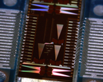
- Wire bonding Kulicke and Soffa
- size < 3 pouces
- 50 µm gold and Al wires
|
Control- 2 optical microscopes
- Contact profilometer Tencor
- Probe station (I(V))
|