


Context
OPTOSI seeks to demonstrate disruptive pathways towards the integration of III-V-based photonic functionalities on a single chip for optical interconnects. The work program will be based on the investigation and evaluation of the direct molecular-beam epitaxy of III-V compounds on silicon substrates following two complementary routes : the III-Sb LMM approach and the GaP(N) QLM approach :
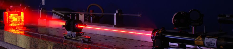
![]() A metamorphic approach based on the peculiar stress-relaxation properties of the III-V coumpounds highly mismatched. Relaxation occurs by formation of a dislocation network confined at the III-V/Si interface, leading to a weak threading defects density ;
A metamorphic approach based on the peculiar stress-relaxation properties of the III-V coumpounds highly mismatched. Relaxation occurs by formation of a dislocation network confined at the III-V/Si interface, leading to a weak threading defects density ;
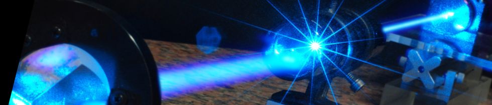
![]() A quasi lattice-matched approach based on GaP-based compounds leading to misfit-dislocation-free GaP/Si interface.
A quasi lattice-matched approach based on GaP-based compounds leading to misfit-dislocation-free GaP/Si interface.
Both these platforms will be used to grow laser heterostructures including either III-Sb or GaP(AsN) compounds in order to evaluate the potential of both approaches in the Si photonics framework.
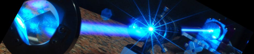
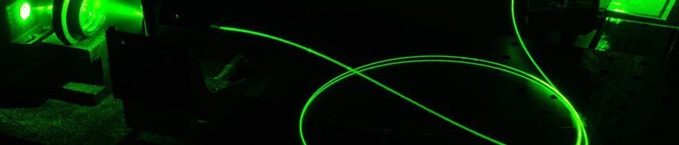
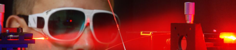
New nanostructures will be explored, using both approaches, for the light emission in the 1.2 - 1.5 µm range, suitable for the optical interconnections, from the large wavelengths concerning the III-Sb approach and the low wavelengths concerning the GaP(As,N) one.
OPTOSI brings together four 4 academic partners (IES, Foton, LPN, LPCNO) with complementary expertise covering the material sciences, physics and technology of laser devices. The consortium is completed by an industrial partner (II-V lab) for the benchmarking activity.
In case of success the project will have a tremendous impact, well beyond the Si photonics segment, in the whole semiconductor field. This know-how will have a large impact well beyond the Si-photonics field since it will open the way to the integration of any kind of III-V devices on Si, such as MOS transistors expected on the ITRS roadmap or high efficiency solar cells.
The importance of the field is reflected by the fact that the next Compound Semiconductor week, a large professional event which aims at “defining the next steps for the compound semiconductor industry”, will be dedicated to integration of III-Vs with Si (http://www.cseurope.net).
Goals
The main objectives and routes of OPTOSI are :
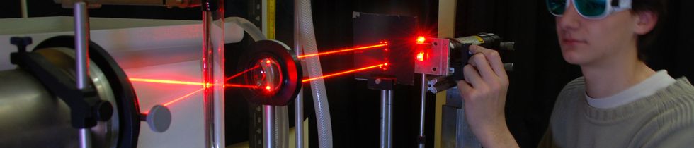
![]() The development of III-V/Si epitaxial platforms following two routes : the III-Sb LMM approach and the GaP(N) LM approach.
The development of III-V/Si epitaxial platforms following two routes : the III-Sb LMM approach and the GaP(N) LM approach.
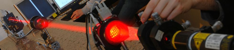
![]() The development of new GaSb- and GaP- based nanostructures for laser active zones emitting in the 1.1 – 1.5 µm wavelength range where Si is transparent and Ge detectors are most efficient.
The development of new GaSb- and GaP- based nanostructures for laser active zones emitting in the 1.1 – 1.5 µm wavelength range where Si is transparent and Ge detectors are most efficient.
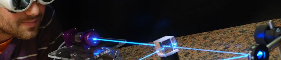
![]() The demonstration of III-V lasers grown directly onto Si wafers.
The demonstration of III-V lasers grown directly onto Si wafers.
Scientific Production
 see in HAL
Partners
III-V lab – IES – LPN – LPCNO
(groupe(s) Foton impliqué(s) : OHM)
Coordinator
IES (Eric TOURNIE)
(person in charge at Foton : Olivier DURAND)
Funding
ANR : 708 k€ (221 k€ included forFoton-OHM)
Voir en ligne :
![]()