


Context
The aim of the project is to provide low-cost and high efficiency tandem cells grown on crystalline silicon (c-Si) substrates, with merging both the monocristalline Si approach with the high-efficiency monocristalline multijunction approach based on III-V materials.
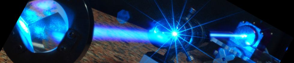
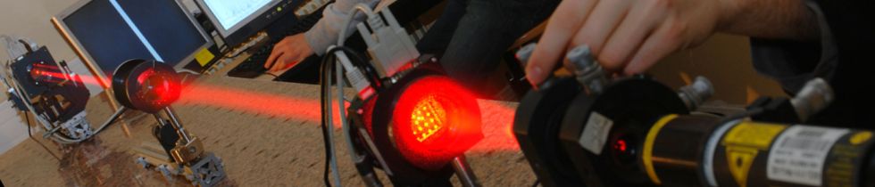
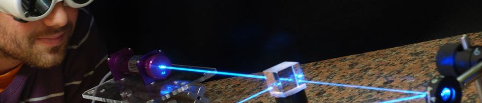
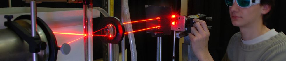
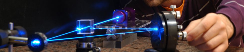
These CPV cells will be used under natural lighting and under low light concentrators (100 suns) developed by IRDEP-CNRS, and benchmarked under medium concentration by HELIOTROP SAS.
The PV cells efficiency is one of the most important parameters for the final cost of electricity, since it impacts directly the ratio between produced energy and production cost. With 22% efficiency modules based on c-Si, the technology seems to reach its limits. To increase further the efficiency of c-Si cells and modules, going to multijunction devices (association of two different absorbing layers in the same cell) seems to be the obvious choice.
While many projects tend to focus on all silicon technology, best high bandgap cells are yet based on III-V compounds. This project proposes to demonstrate the proof-of-concept for a monolithic integration of high efficiency multijunction CPV device on a low cost monocristalline silicon substrate upon which a III-V lattice-matched material will be grown using MBE.
This Lattice-Matched heterostructure with its very low structural defect densities (Dislocations, AntiPhase Domains, point defects) will be capable of sustaining III-V high performing PV devices onto silicon with long life-time.
This novel route overcomes the problems of high cost substrates (as compared to Ge or III-V substrates used currently for this kind of CPV), the killer structural defect formation and reliability issues of lattice mismatched systems (metamorphic approach) and the low reliability and low lifetime of hybrid techniques (such as wafer bonding).
The integration of photovoltaic functions onto a single silicon substrate will also achieve a reduction in the use of III-V based semiconducting materials in high-efficiency multijunction CPVs.
Goals
The two main scientific and technologic objectives of the project are :
- The achievement of GaAsPN (1.7 eV) single cell on Si (with a 15% efficiency under low concentration, i.e. 100 sun).
- The demonstration of a high efficiency and low cost multi-junction solar cell : GaAsPN pn cell at 1.7 eV on Si pn cell at 1.1 eV (25% efficiency under low concentration, i.e. 100 sun, as a first step towards very high-efficiencies >30%)
Lattice-matched layers and slightly tilted substrates are used to overcome the two main difficulties faced by the growth of III-V materials on silicon substrates : misfit dislocations and antiphase lattice defects, in order to obtain defect-free III-V materials and to get large minority carrier diffusion lengths for the PV applications.
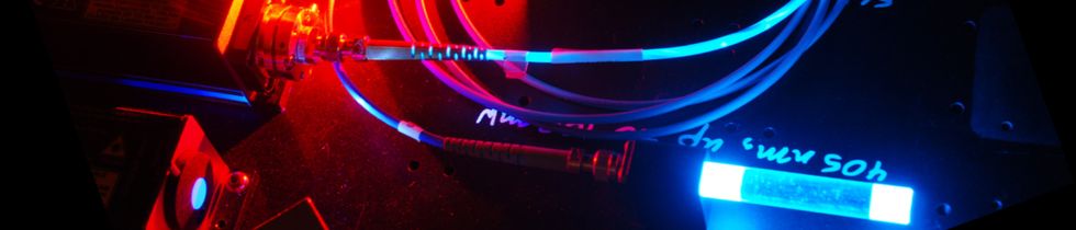
The PV devices will consist in high efficiency tandem cells III-V/Si double-pn-junctions separated with a Buried Tunnel Junction.
The final structure will include a first bottom Si pn (1.1eV low gap) grown on the Si substrate, then a thin GaP layers is grown by MBE to prevent structural defects formation, a top cell GaAsPN pn (1.7eV large gap) junction is then grown on top of it.
The project relies on a high quality consortium which brings together six french partners, and an associated European partner, with high, established competence and complementary methodology and expertise in their fields and leading appropriate workpackages : FOTON (growth of III-V materials), INL (Si-based PV technology), CEMES-CNRS (structural characterizations), IRDEP-CNRS (research in PV development), EDF R&D (a European leader in the Energy sector), HELIOTROP (French manufacturer of HCPV modules) and AALTO (a Finnish associated academic partner specialised in point defects analysis).
The partners are active in European research consortia and in networks of excellence and they drive many projects on the national and international level.
Scientific Production
 see in HAL
Partners
CEMES-CNRS – EDF R&D – IRDEP-CNRS – INL
(Foton groups : OHM)
Coordinator
Foton (Olivier DURAND)
Funding
ANR : 900 k€ (dont 284 k€ pour Foton)
Voir en ligne :
![]()